-
 2021/08/23
A safe distance from including the electrical clearance (distance), creepage distance (creepage distance) and insulat...
-
 2021/08/23
1, FR – 4 sheet is a kind of epoxy plate, has high mechanical properties and dielectric properties, good heat r...
-
 2021/08/23
North American car market is leading the global networking, PCBA OEM generation material predicts 2025, American domi...
-
 2021/08/23
1, brush paint anti-corrosion protection must be tested before the PCBA assembly, inspection, and after a thorough cl...
Collect now! A useful PCB final checklist!
Release time:2018/08/09 news viewed:1149
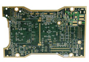
For the novice, after the PCB design is completed, the DRC will have no problem. It is ready to be produced by the GERBER manufacturer. Even if the GEBRER does not come out, the PCB original image will be sent directly to the manufacturer for production, which will be very easy to make mistakes. Therefore, Xiaobian shared the PCB CHECKLIST made by Shangyu Shonway and shared the experience summarized in many years of practice.
PCB structure
1. PCB outline size and positioning hole position.
2, the height of the entire board components.
3. Location and packaging of external interface components.
4. Lead the position and package of the cable.
5. Whether the PCB design meets the limit map requirements.

These are easy to understand, the PCB dimensions, the location of the locating holes, the location of the external interface components are all to be done when you want to do it. The best way is to print out the ratio of 1:1 and then use scissors. Cut it out, cut out the hole and put it on the case, so that it will be clear and white. Anything that is wrong will be seen.
The limit map mentioned in the fifth point is that sometimes, the whole machine casing will have some prohibited wiring areas, or there is fear of friction, or short circuit, some areas can not be wired and copper, these places should pay attention to .

Routine inspection
1. DRC inspection.
2. Have you corrected the problems that occurred in the previous trial production report?
3, left and right or left and right to leave the 5MM process side, in the process side can not put the chip components, because the board size is limited, leaving the process side when left or right or up and down plus 5mm process side. Also make a puzzle chart file.
4. Add a positioning hole with a diameter of 3mm to at least three corners of the PCB.
5. Whether the TQFP with pin pitch less than 0.5mm is placed at the four corners of the whole board (at least two diagonal lines) and around the BGA, and the optical positioning point is placed diagonally on the SOP chip.
6, place the company logo, model, version, date and other silk screen.
7. Whether the place where the wiring is prohibited in the structure limit map meets the requirements.
8, each socket, cable interface to identify silk screen.

Brief explanation
Article 1 This is a must. If you don’t do this, you have not completed the PCB design.
Article 2, whether the problems in the previous trial report were corrected. This article is the product that needs to pay attention to the problem when making the second revision. When doing the second modification of the product, the problem of the previous version must be solved. After the first version is produced, the API engineer must be allowed. That is, the product introduction engineer) lists the problems in production one by one, and solves all the problems of the previous draft when the modification.
Article 3, leaving the 5MM process side left and right or up and down, can not put the chip components in the process side. Due to the size of the board, there is no 5mm process side left or right or left and right when the process side is left. Also make a puzzle chart file. This is for the sake of patch production. When the top placement machine is produced, the board is placed on a track, so there is no patch component at both ends of the rail, as shown in the blue box below. These two sides must be left 5mm, and there is no patch component within 5mm. If you can’t leave it, you need to add another process, use V-CUT.
In Article 4, a positioning hole with a diameter of 3 mm is added to the three corners of the PCB. It must also be noted that if the small board does not matter, the large board must be placed. The three holes have a hole diameter of 3 mm. This is the PCB production, when the board is connected to the electrical test, the fixed board is used, and the electric test cannot be done without adding it.
Article 5, whether the TQFP with pin pitch less than 0.5mm is placed around the four corners of the whole board (at least two diagonal lines) and around the BGA, the optical positioning point is placed diagonally on the SOP chip. It is the optical positioning point, which is the MARK point. This is the placement of the placement unit according to the MARK point when the placement machine is in production. There are at least two diagonal MARK points on the four sides of the whole side. There are two MARK points on at least the diagonal of the four corners of the chip with tight chip pins, such as chips with a pitch of 0.5 mm or more. This will make positioning more accurate for large boards.
Article 6 is to identify the model and version of this product, this is for later traceability.
Article 8 Each socket and cable interface shall be marked with silk screen. It is said that some cables, such as the serial port, identify the function of each pin, as shown in the figure below.
This is the serial port debugging port. There are five pin headers. In the silk screen layer, these five pin headers must be marked for easy debugging. The interface that identifies it should be carefully checked to see if it should be identified.
DFM, EMC, electrical performance
1. Whether the PCB design rules are in line with the board’s process capability.
2. The engineering confirmation problem of the previous version of the PCB manufacturer can be changed in the design.
3. Whether the plug-in device grounding mode is a thermal pad.
4. Is the component package correct?
5. Whether there is anti-short-circuit white oil on the back of the plug-in device.

6, whether to add pad tears.
7. Whether to identify the first leg of the chip.

8. Whether the silk screen of the device is correctly placed.
9. Does the diode indicate polarity?
10, three-stage tube, mos tube, etc., the schematic diagram and PCB packaging are not corresponding.

11. The patch around the V-cut slot is parallel to the direction of the split plate.
12, 3mm around the screw column is prohibited from routing.
13. Whether to ensure the consistency of the plug capacitor direction.
14. Is the distance between the bottom chip and the plug-in via hole 2.5mm or more?
15. Is there a solder mask between the chip pins?
16. The chip component is at least 2 mm from the V-CUT line.
17. Has the dead copper been removed?
18. Is there a heat dissipation pad and a heat dissipation via hole on the power chip and the chip with the heat dissipation pad in the middle?
And open the window on the reverse solder mask to help dissipate heat.
19. Have you cut off the ground copper foil from all the layers below the large inductor?
20. Is the final PCB compared to the SCH netlist?
Article 1, whether the PCB design rules are in line with the board’s process capability
It is the process capability of the board factory. We draw a PCB with a minimum line width, line spacing, the minimum line width of your setting, whether the line distance can be made by the board factory, and the minimum aperture, etc., which need to be confirmed with the board factory. You know that your suppliers should also know their process capabilities and set them up when designing the rules.
Article 2, the engineering confirmation of the previous version of the PCB manufacturer, can be changed in the design.
This engineering problem is that when the last manuscript is sent to the board factory for production, the factory will give you a document that you need to confirm. It is some documents that are not certain in production, you need to be sure, such as some you did not pay attention, silk screen The upper solder mask, some useless silk screen, can be deleted, some impedance control, level design, whether they do what you want, and so on.
Whether the grounding method of the plug-in device of the third plug is a hot pad
It is the plug pad grounding that is preferably in the form of a thermal pad. As shown in the figure below, if the copper is fully plated, it will be difficult to solder because of the fast heat dissipation, and it will be soldered. As shown below:
Article 4 is easy to understand, and each package must be guaranteed to be correct. This must also be checked. When you have a new component package to build at the beginning of the design, you should first record which new components are there, and then check one at the end of the plot.
Whether there is anti-short-circuit white oil on the back of the 5th plug-in device. This is a problem that needs attention when mass production. A silk screen is added between the two pads of the solder layer, which can effectively block the soldering short circuit of the two pads, as shown in the following figure:
Here, on the reverse silk screen layer, a silk screen is added between the two pads, which has some effect on preventing solder short circuit.
Article 6 Whether to add pad tears, this pad teardrop, as shown in the following figure, the line drawn from the pad is thickened to prevent the pad from being soldered many times and the lead is broken.
Article 7 means that each chip must identify the first leg so that the welder does not weld the fault.
Article 10, three-stage tube, mos tube, etc., the schematic diagram and PCB packaging are not corresponding. That is, the triode has three legs. The three pins of the PCB package are corresponding to the three legs in the schematic diagram. In the past, such a problem has been encountered. The three pins of the PCB package do not correspond to the schematic diagram, and are taken back. The debugging is wrong. If you find this problem, you can only use the flying wire to solder the triode. This must be done. One method is that the triode has a standard. It is usually done with the standard diagram shown below. The pin number must be done according to this, and then the foot of the schematic should correspond to this.
In Article 11, the patch around the V-cut slot is parallel to the direction of the split plate. This means that the patch components around the V-CUT are parallel to the V-CUT slot, so that if the V-CUT slot is manually broken, the solder joints of the patch components will not break. As shown in the figure below, if R117 is placed horizontally, when the left side of the process side is broken, the pad of R177 from the edge of the board is easily cracked.
Article 13, whether to ensure the consistency of the plug capacitor direction. Preferably, the capacitor is in one direction, so that the welder does not insert the wrong one.
Article 14, whether the bottom patch is 2.5 mm or more away from the plug-in via pad. This article means that there should be no patch components at least 2.5mm around the pins of the soldering face insert components. Why? Because the chip component is soldered first, and the component is soldered, the plug component is wave soldered. When soldering, the patch attached to the front must be covered with a cover. The cover and the plug are There must be a safe spacing between the components to cover the chip components and expose the pins of the card components. This cover is called a fixture, as shown below:
Article 15, whether there is a solder bridge between the chip pins. Here we will talk about this solder mask, which is separated by green oil between the two pads, as shown below:
On the left, there is a green oil soldering bridge between the two pads, and a green oil soldering bridge is broken between the two pads on the right side. This can be understood. This green oil soldering bridge is designed to prevent shorting of the pads during soldering. This is very important, especially when mass production is required.
Article 16, the patch component is at least 2 mm from the V-CUT line. When the board is divided by the machine, the cutter has a certain thickness, and if there is a patch component within 2 mm of the V-CUT line on the side of the panel, the cutter head will be touched.
Article 19, whether the ground copper foil of all layers below the large inductor is cut off by the power supply. This output inductor is an output square wave signal, which is very fast. If there is ground below, it will cause noise and make the ground unclean, which will affect the performance.
In the previous: What are the benefits of using precious metals such as gold and silver on PCBs? !
The next article: [Technology] PCB surface treatment process
- About PCBA OEM generation interconnection ...
- PCB industry pattern and development trend
- PCBA board between the shell and safety re...
- What are the benefits of using precious me...
- PCB circuit board factory wastewater treat...
- [Technology] PCB surface treatment process
- Anti-corrosion coating PCBA paint what tec...
- Do you really understand PCB? Take you to ...